Decoding CPU Reviews: A Beginner’s Guide to Processor Terms
CPU reviews are complicated. Before you even get to the performance benchmarks, you have to navigate a maze of terms, like silicon, die, package, IHS, and sTIM. That’s a lot of jargon with little explanation. We’ll define the key parts of a CPU that PC enthusiasts discuss the most.
Please note this isn’t intended to be a deep dive, but, rather, an introduction to common terminology for budding CPU geeks.
Start with the Silicon
More than 10 years ago, Intel shared the basics of how it creates its processors, from raw materials to the finished product. We’ll use this process as a basic framework as we look at the key component of a CPU: the die.

The first thing a CPU needs is silicon. This chemical element is the most common component in sand. Intel starts with a silicon ingot, and then slices it into thin discs, called wafers.
The wafers are then polished to a “mirror-smooth surface,” and then the fun begins! The silicon transforms from a raw material into an electronic powerhouse.
The silicon wafers get a photoresist finish. Then, they’re exposed to UV light, etched, and get another layer of photoresist. Eventually, they’re doused with copper ions and polished. Metal layers are then added to connect all the tiny transistors that exist on the wafer at this point. (As we mentioned previously, we’re only covering the basics here).
Now, we come to the point we care about. The wafer is tested for functionality. If it passes, it’s sliced into small rectangles called dies. Each die can have multiple processing cores, as well as a cache and other components of a CPU. After slicing, the dies are tested again. Those that pass are destined for store shelves.
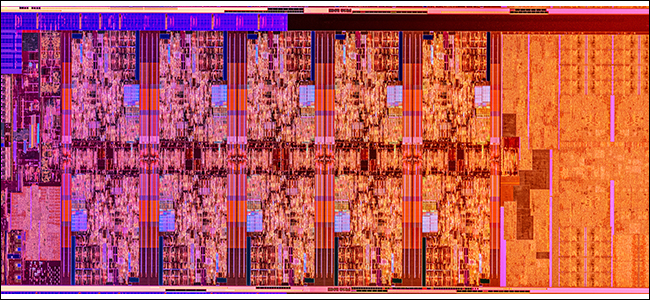
That’s all a die is: a little piece of silicon loaded with transistors that’s the heart of any processor. Every other physical part helps that little piece of silicon do its job.
But, here’s the kicker: depending on the processor you get, a CPU can have either one or multiple silicon dies. One die means all the processor’s components, such as cores and cache, are on that one piece of silicon. Multiple dies have connecting material between them.
There’s no easy way to know for sure whether a particular CPU has single or multiple dies. It’s up to the manufacturer.
Intel is famous for using a single die for its consumer processors. This is called a monolithic design. The advantage of a monolithic design is higher performance, since everything is on the same die and there’s little delay in communication.
However, it’s harder to make advances when you have to pack smaller and smaller transistors onto the same size of silicon. It’s also harder to produce single dies that perform with all cores firing—especially when we’re talking about eight or 10 cores.

This is in contrast with AMD. The company does make some monolithic processors, but it’s Ryzen 3000 desktop series use smaller silicon chiplets, which currently have four cores on the silicon. These chiplets are called a core complex, or CCX. They’re packed together to make a larger Core Complex Die (CCD). That CCD is what counts as a die in AMD’s parlance. It’s several small silicon chiplets that are connected to create a functioning CPU.
AMD processors also have a silicon die separate from the CCDs called the I/O die. We won’t get into the details of that here, but you can read more about it in this June 2019 article from TechPowerUp.
Given how complex it is to create functioning silicon dies, it’s obviously much easier to create a smaller unit of four cores, rather than a single die with 10 cores.
The CPU Package
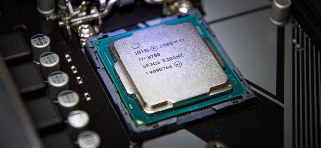
Once the die is finished, it needs some help to talk to the rest of a computer system. This usually starts with a small, green board, often referred to as the substrate.
If you flip over a completed CPU, the bottom of the green board has gold contacts (or pins, depending on the manufacturer). Those contacts or pins fit into the socket of a motherboard and allow the CPU to talk to the rest of the system.
Jumping back inside our processor, we haven’t covered up the silicon die yet. The major component here is the thermal interface material, or TIM. The TIM improves thermal conductivity (important for CPU cooling). It usually comes in one of two forms: thermal paste or sTIM (soldered thermal interface material).
The TIM material can vary between generations of CPU from the same manufacturer. You can never really know what a particular CPU has unless you read CPU news or open (“delid”) a finished processor yourself. For example, Intel used thermal paste from 2012 through ’18, but then started using sTIM on its upper-range, ninth-generation Core processors.
At any rate, these are the pieces that make up the package: the die, the substrate, and the TIM.

Finally, on top of the package, there’s an integrated heat spreader, or IHS. The IHS spreads out heat from the CPU onto a larger surface area to help reduce the CPU’s temperature. The CPU fan or liquid cooler then dissipates the heat building up on the IHS. The IHS is usually made of nickel-plated copper. The CPU’s name is printed on it, as shown above.
That wraps up our tour of the CPU. Again, the die is the bit of silicon that contains the processor cores, caches, and so on. The package includes the die, PCB, and TIM. And, finally, you also have an IHS.
There’s a lot more to it than that, but these are the essentials on which CPU news and reviews tend to focus.


Leave a reply